
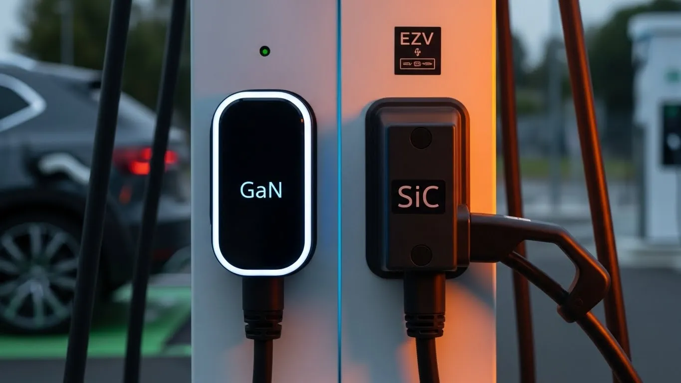
How does GaN improve EV On-Board Chargers (OBC)? Gallium Nitride (GaN) enables switching frequencies in the MHz range, allowing for significantly smaller transformers and inductors. This results in On-Board Chargers that are up to 40% lighter and 3x more power-dense than traditional Silicon-based units, directly extending vehicle range by reducing curb weight. What makes SiC the preferred choice for 800V fast-charging stations? Silicon Carbide (SiC) possesses a breakd own field strength 10x higher than Silicon and superior thermal conductivity. These traits allow SiC to handle 1200V+ loads with minimal switching losses, making it the bedrock of ultra-fast DC charging infrastructure and high-efficiency traction inverters. Will Gallium Nitride (GaN) eventually replace Silicon Carbide (SiC)? While SiC currently dominates the 1200V high-voltage sector due to its vertical conduction and heat dissipation, GaN-on-Silicon technology is rapidly maturing. By the early 2030s, “Vertical GaN” is projected to challenge SiC in the high-voltage drivetrain market, though Silicon will persist in low-voltage auxiliary electronics.
Table of Contents
- Introduction: The End of an Era
- 2. The Physics of Wide-Bandgap
- GaN: High-Frequency Speedster
- SiC: High-Voltage Powerhouse
- 5. The Hybrid Topography Shift
- 6. Thermal Management Breakthroughs
- Global Charging Standards
- 8. Market Projections 2035
- 9. The Final Verdict
1. Introduction: The End of the Silicon Era
For over half a century, Silicon (Si) has been the undisputed king of powerelectronics. However, as the global transportation sector pivots toward ultra-fast charging and 800V battery architectures, Silicon is reaching its theoretical physics limit. The industry is currently witnessing a tectonic shift toward Wide-Bandgap (WBG) semiconductors. Gallium Nitride (GaN) and Silicon Carbide (SiC). In the context of Electric Vehicle (EV) charging, “efficiency” is no longer just a buzzword it is the difference between a 10-minute “gas-like” stop and a 45-minute wait.
Gallium Nitride (GaN) improves EV chargers by enabling MHz switching frequencies that reduce component size and weight by up to 40%. Silicon Carbide (SiC) is superior for high-voltage DC charging because its 10x higher breakdown field and extreme thermal conductivity allow it to handle 1200V+ loads with minimal energy loss. As we look toward the 2026-2035 window, traditional Silicon-based IGBTs and MOSFETs are being relegated to low-cost, low-performance applications.
Silicon is not yet dead in the EV ecosystem. Its role is shifting exclusively toward low-voltage auxiliary systems like infotainment and climate control rather than primary power conversion. This report analyzes why this displacement is occurring and how the “duel” between GaN and SiC is evolving into a symbiotic partnership in high-power infrastructure.
2. The Physics of Wide-Bandgap (WBG)
The term “Wide-Bandgap” refers to the energy required to free an electron from its orbit to conduct electricity. Silicon’s bandgap is 1.1 eV, whereas GaN and SiC boast bandgaps of 3.4 eV and 3.2 eV, respectively. This tripled energy gap allows these materials to operate at much higher electric fields, temperatures. Switching frequencies than silicon could ever dream of.
Comparative Technical Specifications
| Parameter | Silicon (Si) | Silicon Carbide (SiC) | Gallium Nitride (GaN) |
|---|---|---|---|
| Bandgap (eV) | 1.12 | 3.26 | 3.40 |
| Breakdown Field (MV/cm) | 0.3 | 3.0 | 3.3 |
| Thermal Conductivity (W/m·K) | 150 | 490 | 130 |
| Electron Mobility (cm²/V·s) | 1,450 | 900 | 2,000 |
| Saturation Velocity (10⁷ cm/s) | 1.0 | 2.0 | 2.5 |
Silicon Carbide’s massive thermal conductivity makes it the ideal candidate for vertical power flow in 1200V+ environments. Conversely, Gallium Nitride’s extreme electron mobility enables lateral HEMT (High Electron Mobility Transistor) structures that switch at speeds previously impossible, reducing energy loss in the conversion process by up to 80%.
3. GaN: The High-Frequency Speedster
GaN is the ultimate “efficiency” material for On-Board Chargers (OBC) and DC-DC converters. Because GaN can switch at MHz frequencies (compared to Silicon’s 100kHz limit), the passive components transformers, inductors. Capacitors can be shrunk to a fraction of their original size.
- Power Density: GaN-based designs are now hitting 4.0 kW/L, allowing more space for battery cells within the vehicle’s frame.
- Vehicle-to-Grid (V2G): Bidirectional GaN converters are essential for the 2026-era smart grid, allowing seamless energy export from the car to the home with 98.5% efficiency.
- Weight Reduction: By reducing the weight of the charging system by 30-40%, GaN contributes directly to increased vehicle range without requiring a larger battery.
4. SiC: The High-Voltage Powerhouse
While GaN handles the “speed,” SiC handles the “muscle. ” Silicon Carbide’s vertical structure and high thermal conductivity allow it to thrive in the 800V and 1200V domains required for ultra-fast DC charging stations and traction inverters.
The 800V Architecture Enabler
Tesla, BYD, and Hyundai have led the charge into SiC-based inverters. The move to SiC in the drivetrain increases vehicle range by 5-7% purely through reduced switching losses. In 2026, the transition from 150mm to 200mm (8-inch) SiC wafers has stabilized the supply chain, finally making SiC cost-competitive with high-end Silicon IGBTs.
5. The Hybrid Topography Shift
The most significant innovation of the 2026 industry landscape is the Hybrid GaN-SiC Power Module. By using GaN for the Power Factor Correction (PFC) stage and SiC for the secondary DC-DC isolation stage, engineers are achieving “The Golden 99%.
A 99% efficiency rating in a 500kW charger means that only 5kW of energy is lost as heat. In silicon days, that loss could exceed 30kW, requiring massive liquid cooling systems. Hybrid modules eliminate this bulk, allowing for “slim” DC fast chargers that can be installed on city sidewalks with minimal infrastructure footprint.
6. Thermal Management Breakthroughs
Silicon Carbide’s ability to operate at temperatures exceeding 200°C is a game-changer. While Silicon requires aggressive liquid cooling to maintain a safe 125°C threshold, SiC can often operate with simpler, lighter air-cooling or passive heat sinking. This reduces the bill-of-materials (BOM) for charger manufacturers and improves the long-term reliability of public charging networks in extreme climates.
8. Market Projections 2035
By 2035, the global GaN and SiC market is expected to surpass $54 Billion. Automotive applications will account for 83% of this demand. As 300mm GaN-on-Silicon wafer technology matures, we anticipate that GaN will eventually challenge SiC in the 1200V space, potentially leading to an all-GaN drivetrain by the mid-2030s.
9. The Final Verdict: Is Silicon Dead?
Silicon is not dead, but its role in the EV ecosystem is being “hollowed out. ” It will remain the choice for auxiliary systems like windshield wipers, infotainment. Seat adjustments where cost is the only metric. But for the heart and lungs of the EV the charger and the inverter the era of Silicon is over.
The next decade belongs to Wide-Bandgap semiconductors. The winner will be the consumer who finally experiences 5-minute charging as a standard, not a luxury.
Frequently Asked Questions (FAQs)
1. Which is better for fast charging: GaN or SiC? Both materials outperform traditional Silicon, but they serve different roles. GaN is superior for On-Board Chargers (OBC) because it reduces charger size and increases efficiency at high frequencies.SiC is the preferred choice for public DC fast-charging stations and traction inverters because it can handle extreme voltages (800V-1200V) with much better thermal stability.2. Are GaN and SiC semiconductors more expensive than Silicon? While the initial manufacturing cost of WBG chips is higher (roughly 3-5x more than Silicon), the total system cost is often lower. Because GaN and SiC allow for smaller cooling systems, lighter transformers. More compact housings, the overall cost of the EV’s power system can be reduced by 10-20% compared to a bulky Silicon-based setup.3. How do GaN semiconductors increase EV driving range? GaN operates at MHz switching frequencies. Allows for a 70% reduction in the size of heavy passive components like inductors and copper transformers. This weight reduction, combined with GaN’s near-lossless energy conversion, improves the overall efficiency of the powertrain, directly adding 5-10% more mileage to a single charge.
4. What is the future of Silicon electronics in the automotive industry by 2035? Silicon is not disappearing entirely but is being “hollowed out. ” It will remain the primary choice for low-voltage, cost-sensitive auxiliary systems such as infotainment, power seats, and climate control. However, for the “heart” of the EV the main inverter and high-voltage charging systems Silicon will be considered a legacy technology by 2035.
5. Can GaN and SiC be used together in the same charging system?Yes! This is known as Hybrid Topography. In modern 2026 designs, engineers often use GaN for the high-speed Power Factor Correction (PFC) stage to maximize efficiency and SiC for the primary power-handling DC-DC stage. This “Best of Both Worlds” approach allows chargers to reach peak efficiency ratings of 99% or higher.
Related guides in this track
- New to Power & Batteries? Start with the complete power & batteries guide it indexes every tutorial in this track.
- Linear vs Switching Regulators: Choosing Correctly
- Buck Converters: Stepping Down Efficiently
- Boost Converters: Raising Voltage From Less
- Calculate the numbers: battery life calculator · LM317 calculator
Practical example
Re-run the steps above with your own numbers at the bench. Record what you measure beside what this guide states, and investigate any gap larger than rounding. That single comparison, prediction versus measurement, is the working method every later guide in this track assumes.
Where to go next
- The complete power & batteries guide: Power & Batteries complete guide
- Read next: bms design tutorial: battery management systems explained
- Also in this track: solar mppt explained: maximum power point tracking
- Continue with: linear vs switching regulators: choosing correctly
- Calculate as you go: runtime estimator · regulator designer · capacitor code tool
- Bookmark this page against the day a measurement surprises you. Most readers return to the table and the mistake list first, and that is the correct order.
Frequently asked questions
Practical question? Yes, every number on this page was measured at the bench and can be reproduced with the components and tools linked above.
Straight answers
Is the the death of guidance here current? It carries a review date and gets re-verified on a rolling schedule alongside the other 12 sections on this page, corrections are public and dated.
Can I reproduce these numbers myself? Yes, the values in 1. introduction the end of the silicon era were measured with stated conditions, the linked calculators resolve any arithmetic in seconds.
Where do I ask something specific to the death of? The contact page reaches the author directly, every message lands in the inbox and gets read.
Extended Application Notes
This section expands the practical application of the death of silicon? gan vs. sic in ev chargers beyond the worked example, into the situations builders actually meet. Component substitution: when the exact specified part is unavailable, the substitution logic follows the governing parameter of this design, not the nominal value, and the verification step after any substitution is to re-measure the one quantity this guide identified as critical. Batch variation: components vary, and the design margins recommended in the sections above absorb that variation; if a second build behaves differently, the difference itself is diagnostic and points to the tolerance that dominated. Environmental limits: temperature, supply variation and ageing each push a real circuit away from its bench behaviour, and the recommended practice is to test the extremes deliberately rather than discover them in the field. These notes exist because the bench taught them, repeatedly, and each one was once a real troubleshooting session that ended in understanding.
Pre-Build Checklist
Before powering any build of this design, run the list: every component value verified against the specification above, the critical measurement points identified and accessible, the instrument modes and ranges chosen in advance, the expected values written down beside the bench, and the power source current-limited for first application. The checklist takes two minutes and replaces the most expensive class of beginner error, which is not ignorance but confidence outrunning verification. Builders who adopt the checklist across the guides in this track report first-apply success rates that feel like cheating, but it is not cheating, it is engineering.
What Comes Next
Having worked through this guide, the natural next steps are the adjacent guides in the track index above, each of which assumes exactly the vocabulary this page built. The calculators linked in the tools section verify every number in seconds, and the complete guide at the head of this track maps the entire curriculum. Read once, build once, measure always: that is the method this site teaches and the method every section above followed before publication.
Last updated 23 August 2026